TSMC, Samsung, and Intel agreed to accelerate the transition to new lithographic technologies
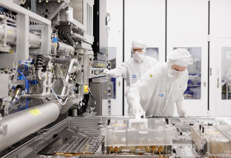
- TSMC, Samsung, and Intel are jointly transitioning to High-NA EUV equipment
- The size of photomasks will increase from 150 to 300 millimeters
- The throughput of scanners will increase by 40 percent
- Samsung will implement the technology in 2028, TSMC in 2030
The semiconductor industry is preparing for a large-scale modernization of manufacturing processes. Taiwanese company TSMC, South Korean Samsung, and American Intel have agreed to implement advanced lithographic technologies that should significantly accelerate the development and production of next-generation chips.
A key element of this collaboration is the transition to High-NA EUV (extreme ultraviolet radiation with high numerical aperture) equipment and the increase in the size of photomasks—special templates used for designing chips on silicon wafers. Traditionally, photomasks were 150 millimeters in size, but the industry is preparing to double this parameter to 300 millimeters.
Such a transition was long considered economically unfeasible due to the high cost of equipment and the complexity of implementation. However, coordinated actions by all major manufacturers will allow for the distribution of the investment burden and make modernization more accessible for the industry as a whole. Representatives of ASML, the supplier of lithography equipment, note that increasing the size of photomasks will enhance the throughput of scanners by 40 percent and simplify the chip design process.
Innovation implementation schedule
Intel is a leader in the application of High-NA EUV technology. The company has already transitioned from prototypes to selective use of such equipment in the mass production of Panther Lake processors using Intel 18A technology. The American manufacturer has also actively promoted the shift to larger photomasks over the past three years.
Samsung plans to start using High-NA EUV equipment for memory production in 2028. The company will collaborate with industry partners when implementing new photomasks, but specific timelines for this migration are not provided.
TSMC, the largest contract chip manufacturer in the world, is moving more conservatively. The company will start using High-NA EUV equipment in 2030, but will initially combine it with traditional 150-millimeter photomasks. A pilot production line for larger photomasks (300 mm) is planned to be launched in 2031, and their use in mass production will only begin in 2033.
Significance for the industry
The Dutch company ASML introduced low numerical aperture EUV equipment back in 2019, and then spent many years preparing to launch high numerical aperture systems. The current agreement among three giants of the semiconductor industry to jointly transition to new technologies gives momentum to the development of the entire chip manufacturing ecosystem.
Such modernization will allow the industry to create more powerful and advanced microchips needed for the growing demand for artificial intelligence, cloud computing, and other high-tech applications. The coordinated approach of the major manufacturers should accelerate the achievement of target metrics and reduce overall costs of innovation implementation.
Source: 3DNews